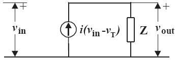
Fig. 5.50. Circuit representation of the model
The design of electronic and telecommunication integrated circuits is unavoidably faced with simulation of analogue subsystems of ever rising complexity thereby building more complex mixed-signal systems containing both analogue and digital parts. Design of such systems needs simulation tools that perform fast and accurate in the same time. Main obstacle to this requirement is related to the difficulties in high level modeling of the analogue part and accurately enough modeling of the digital-analogue (D/A) and analogue-digital (A/D) interfaces being frequently encountered in such systems. In fact at the (D/A) interface one needs to model the output circuit of the digital part in order to enable electrical excitation for the analogue load. In the opposite case, at the (A/D) interface, we need to model the input impedance of the digital part in order to establish conditions for computation of the voltage and current at the interface. Having in mind that the simulation is performed in the time domain, the fact that we are dealing with mixed-level simulation, and the complexity and non-linearity of the circuits involved, one generally applies behavioral modeling for these purposes.
We will consider here the situation when the signal is transmitted from the logic to the analogue element, and then we need digital to analogue conversion. Since the load is analogue, there is a problem in generating of the signal waveform on the output of the digital circuit. Modeling of D/A node is very complex because one needs to get the waveform of the signal that drives the analogue part of the circuit out of the set of logic states. The conversion algorithms are mostly based on the synthesis of the electronic circuit that replaces the logic element, and that is applied as excitation to the actual node. The propagations of the logic elements should also be considered.
The following solution is based on artificial neural networks. It is considered very convenient because the function is approximated using the measured values, and no electronic circuit synthesis is needed.
A new topology of the circuit is proposed for this purpose, being depicted in Fig. 5.50.
Fig. 5.50. Circuit representation of the model
An inverter is considered here, and v in stands for a controlling ramp-shaped voltage-waveform,
and Z is a time delay recurrent neural network approximating the function
I max is the maximal supply current during the transition in the inverter, and v T is (usually) equal V DD/2, V DD being the supply voltage. Obviously, the ANN model of Z has one input (current) and one output (voltage) terminal. The training of the network is performed based on training pairs (i(t), v out(t)), where i(t) is calculated from (5.12) while v out(t) is obtained from simulation of the circuit to be modeled (here inverter). The neural network is a time delay recurrent network (Z), with one hidden layer, five input, three hidden and one output neuron.
Inverter has only one input, so the value of v in voltage is only one. When we are dealing with multi-input circuits, there exist more input voltages because for every combination of inputs there is corresponding output impedance. Also, there is a problem with sequential circuits because the output state depends on input states, as well as on previous output state. During the logic simulation, there always exists information about the events and time of their happening, so it is known what inputs caused certain state and which impedance should be applied to the certain node.
The first results are shown in Fig. 5.51. Here output waveforms of the original inverter and the model are shown in order to show the quality of the approximation procedure. Unloaded circuits are simulated. A behavioral simulator, Alecsis is used to exercise such model.
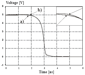
Fig. 5.51. Digital-analogue interface modeling a) response of an unloaded CMOS inverter (considered as digital output) and b) of the new model
The following three examples are intended to check the modeling procedure based on situations not present during the training procedure. Fig. 5.52 represents two responses. The first trace is the output voltage of an inverter (all modeled by regular transistor models) being loaded by inverter. The second one represents the response of the same circuit with ANN model used for the driving part and circuit model for the loading. This situation was unknown in the modeling process.
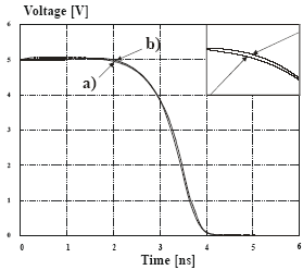
Fig. 5.52. Digital-analogue interface modeling. a) response of an inverter loaded by inverter and b) of a model loaded by inverter
Further, Fig. 5.53 represents similar comparison the loading element being a transmission line modeled by a -RC network.
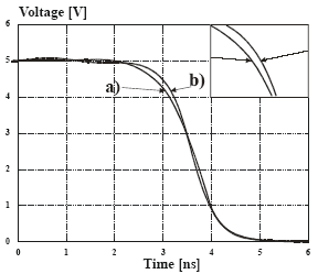
Fig. 5.53. Digital-analogue interface modeling. a) response of an inverter loaded by RC -network and b) of a model loaded by RC -network
Finally, a diode load was used to demonstrate the successfulness of the ANN model in the case of “large” non-linear dynamic load. The comparison of the circuit simulation and behavioral simulation are given in Fig. 5.54.
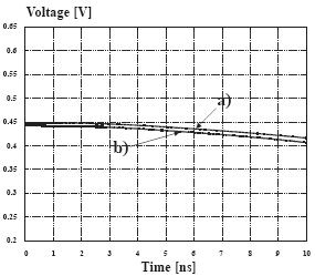
Fig. 5.54. Digital-analogue interface modeling. a) response of an inverter loaded by diode and b) of a model loaded by diode